-1
$\begingroup$

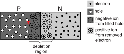
In this image: enter image description here

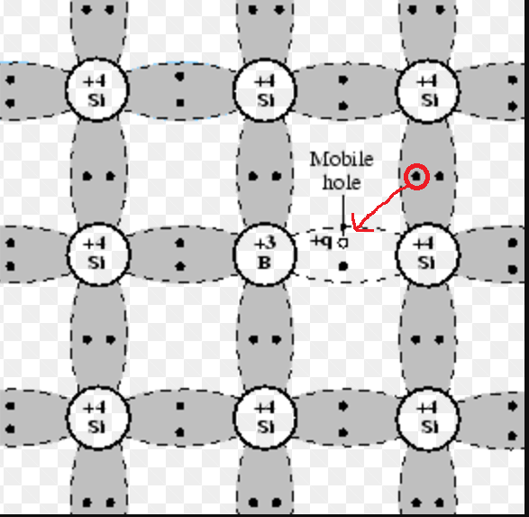
Can the following electron take up 'hole'? If so, this question is sort of leading onto a bigger question about PN junctions.

enter image description here

What is preventing the electron in the ion from moving to the next hole?

Is it to do with the strength of the covalent bond being stronger than that of the more positive charge in the hole?

Edit: What I'm trying to understand is why can't the extra electron in the negative boron ion, take up the holes to the left of it in the P (where I've drawn the red arrow in the 2nd diagram). Shouldn't that then allow another conducting electron to take up the hole in the positive ion? And can't this process keep happening till it's fully diffused? I'm still learning all this, this question is more out of curiosity.

$\endgroup$
7
  • 4
    $\begingroup$ Well, that is how holes move. $\endgroup$
    – Jon Custer
    Commented May 7, 2017 at 15:25
  • $\begingroup$ I don't understand what you are asking. Electrons from covalent bonds are the ones that delocalized holes. Energy level of acceptor impurity is close to valence band energy, which permits electron from a nearby covalent bond to fill it, and remove hole. $\endgroup$ Commented May 7, 2017 at 15:25
  • $\begingroup$ @PrittBalagopal Can you explain how the PN junction works then? What's stopping the electron on the ion from moving to the hole like you said? $\endgroup$
    – Physco111
    Commented May 7, 2017 at 23:46
  • $\begingroup$ @Physco111 PN junctions have conduction electrons in n side fill up the holes in p side. $\endgroup$ Commented May 8, 2017 at 2:54
  • $\begingroup$ @PrittBalagopal So why then does a PN junction even exist? Shouldn't all the conduction electrons in the N side take up all the holes in the P side? $\endgroup$
    – Physco111
    Commented May 8, 2017 at 15:22

1 Answer 1

2
$\begingroup$

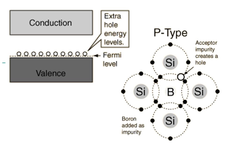
When you dope a pure semiconductor like silicon with boron, a few silicon atoms are replaced with boron atoms. Boron, being a trivalent impurity, can only form 3 bonds with the nearby silicon atoms, but what about the fourth bond? A vacancy for an electron is created over there, and is called a hole.

enter image description here

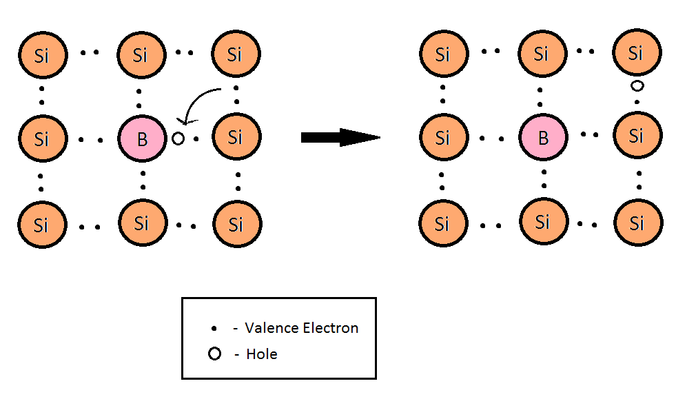
This hole isn't going to stay there. The energy of the acceptor impurity atom (and of the hole) is often so close to the energy level of the valence electrons, that a nearby valence electron can fill up that hole, and move the hole to the initial location of the nearby electron. See this picture that shows holes moving:

enter image description here

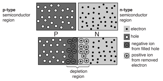
As a follow up, a p-n junction consists of two semiconductor wafers pasted on each other, one being of n-type, and the other of p-type. It would look something like this: enter image description here

The conduction electrons, as you have pointed out, do have a tendency to migrate to the p-side, and will fill up the holes. By doing so, these electrons move from the conduction band on the n-side, to the valence band on the p-side. This movement, however, makes the p-side negatively charged, and the n-side positively charged. An electric field develops in between, which opposes this natural migration of electrons. Ultimately, a field forms strong enough to block all the electrons trying to cross the junction. The potential difference between the junction is called barrier potential, which is about 0.7V for silicon, and 0.3V for germanium.

$\endgroup$

Your Answer

By clicking “Post Your Answer”, you agree to our terms of service and acknowledge you have read our privacy policy.

Not the answer you're looking for? Browse other questions tagged or ask your own question.